オックスフォード・インストゥルメンツー事業部ページ
シリコンカーバイド (SiC) は、高電力用途デバイスに対して適した電子的および物理的特性を有しています。また、高速スイッチング、高出力RFデバイスを可能にする高品質の窒化ガリウム (GaN) を成長させるための基盤としても使用されます。SiC は誘導結合プラズマエッチング (ICP) を使用してエッチング、プラズマ CVD (PECVD) や誘導結合プラズマ CVD (ICPCVD) によりデポジションが可能です。
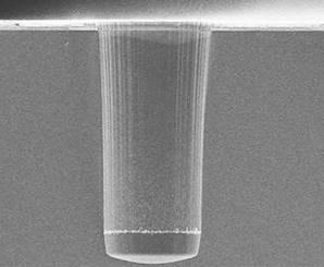
プロセスの専門知識を活用して、欠陥のない表面で高いエッチング速度を実証しました。RF デバイスの Via エッチングで、下層に対する優れた選択性が達成されています。パワーデバイス向けエッチング形状から、過剰なエッチングの無い良好なプロファイル制御が行われていることがわかります。
100%シランや希釈したシランなど、様々な化学薬品を使用できます。
良好に応力コントロールされた高均一性薄膜形成
PH3, B2H6, TMB, TMP を用いたドーピング
100%シランや希釈したシランなど、様々な化学薬品を使用できます。
良好に応力コントロールされた高均一性薄膜形成
PH3, B2H6, TMB, TMP を用いたドーピング

© オックスフォード・インストゥルメンツ 2026