オックスフォード・インストゥルメンツー事業部ページ
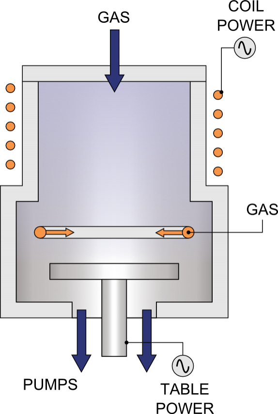
拡張

誘導結合プラズマ化学気相堆積 (ICPCVD)

ICP源における高密度プラズマの生成により、低温において低損傷で高品質の誘電被膜のデポジションを実現する技術です。低温デポジションであるので、温度による影響を受け易い薄膜やデバイスの製造に適しています。

ハイライト

  • イオンエネルギーとイオン流密度の独立制御が可能
  • 代表的なプロセス圧力:1~10 mtorr
  • プラズマ密度:>1011 cm-3
  • プラズマが基板と接触
  • デポジション過程で、イオン流は低エネルギー
  • イオン流(プラズマ密度)は、ICPパワーに依存
  • ESS(静電遮蔽)による、高純度の誘導プラズマ
  • 完全自動ICP(自動同期の2個のRFユニット)
詳細情報についてはこちら
  • 低温で生成した、低損傷で優れた品質の薄膜
  • デポジション可能な代表的な材料:5℃までの低温基板による、SiO2、Si3N4とSiON、SiとSiC
  • ICP源のサイズ65mm、180mm、300mmで、最大200mmのウェハーについて均質な製造が可能
  • 5℃から400℃までの温度範囲に対応可能な電極
  • ICPCVDのガス分布に関する特許技術
  • エンドポイント検知可能な、その場チェンバー洗浄

PlasmaPro 80 PlasmaPro 100
Electrode size  240mm
Wafer size Up to 200mm
Loading  Open Load Load locked or cassette
Substrates 50mm wafers  Up to 200mm with carriers options available for multi-wafers or small pieces
Dopants  No Various dopants available which include PH<sub>3</sub>, B<sub>2</sub>H<sub>6</sub>, GeH<sub>4</sub>
Liquid precursors No
MFC controlled gas lines 8 or 12 line gas box available 
Wafer stage temperature range  20°C to 400°C 0°C to 400°C
In situ plasma clean  Yes

Our ICPCVD cleaning regime was developed to give reproducible deposition and low particles between mechanical cleans

  • Reduced cleaning time
  • Higher utilisation through optional interleaved clean
  • Accurate endpoint resulting in reduced over-etch of chamber components and increasing their lifetime

High Rate Clean Process Features

  • System Utilisation >70%
  • SF6 /N2O gas mixture
  • Improved End Point control
  • Plasma clean results in increased optical intensity with greater endpoint signal/resolution
  • Actual plasma clean time depends on film material, film quality and film thickness

Interleaved Clean Mode 

  • High utilisation
  • Highly repeatable deposition rate
  • Low added particle counts maintained with clean after every wafer
  • > 50 microns between mechanical cleans

ICPCVD Systems