オックスフォード・インストゥルメンツー事業部ページ
Silicon Oxide (SiO2) in its variety of forms is an essential material for semiconductor, MEMs and optoelectronic devices. Quartz is used in gratings for Augmented Reality (AR); Doped oxides are used for waveguides and SiO2 can be used for device passivation. SiO2 may be deposited and etched using several technologies:
The PlasmaPro 100 Polaris brings together unique Electrostatic Clamp (ESC) technology along with our well established Cobra300 ICP source. This delivers excellent repeatability while maintaining high etch rate and profile quality.
Process optimised for excellent control of profile at optimised etching rate.
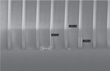
High aspect ratio high quality nanoscale SiO2 etch
Anisotropic and isotropic profile available at competitive etching rate with optimised uniformity.
More on RIE Request more informationExcellent control of profile with expertise in optimising tilt of features.
More on IBE Request more informationExcellent material quality and low damage, even at low deposition temperature.
More on ALD Request more information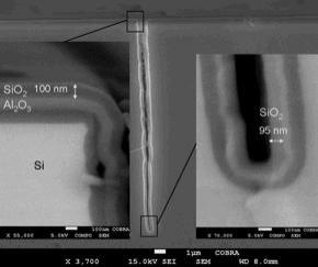
Very high conformality with short cycle time (90 ms prec. and 4.5 s plasma). Courtesy TU/e
Excellent uniformity of both thickness and refractive index, and stress control available at high deposition rate. Different chemistries can be used: pure and diluted silane.
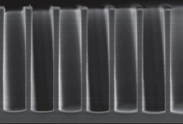
SiO2 deposited using TEOS and O2 by ICP CVD in ~50μm deep trench 4:1 aspect ratio
Excellent uniformity of both thickness and refractive index. Stress control available at high deposition rate. Different chemistries can be used: pure and diluted silane.
More on PECVD Request more information
Excellent stoichiometry with competitive deposition rate.

© オックスフォード・インストゥルメンツ 2026