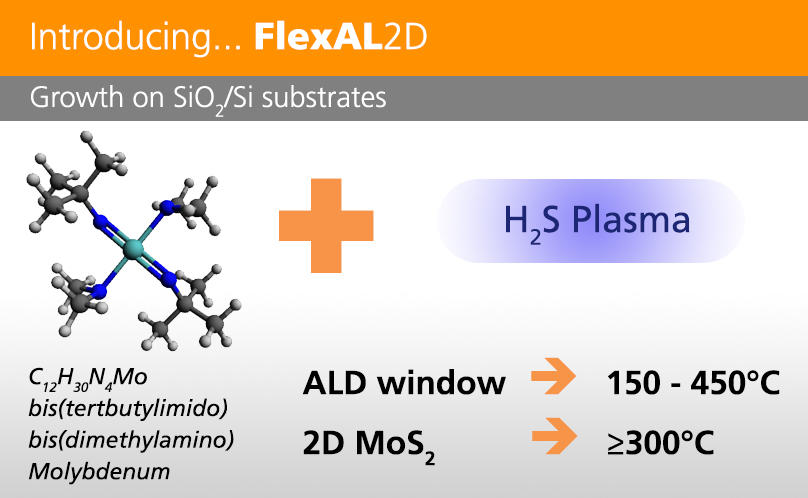
Our ALD and 2D technical specialists have teamed with the Eindhoven University of Technology research teams to realise Atomic layer deposition (ALD) of 2D transition metal dichalcogenides (TMDCs) for nanodevice applications
The FlexAL2D offers a number of benefits for growth of 2D materials:
| 2D materials growth | Robust ALD processes for 2D materials | Tunable morphology |
| At CMOS compatible temperatures | Self-limiting ALD growth | Control over basal plane or edge plane orientation |
| With precise digital thickness control | MoS2: | Growth of ALD dielectrics & other ALD layers on 2D materials in one tool |
| Over a large area (200mm wafers) | Oxygen and carbon free (<2%) | Create advanced 2D device structures |
| High growth per cycle ~0.1 nm/cycle | RF substrate biasing option for film property control | |
| Crystalline material above 300°C |