オックスフォード・インストゥルメンツー事業部ページ
拡張

ダイヤモンド プロセス

Diamond offers a set of characteristics that make it an interesting choice for a wide range of applications. It has the highest known thermal conductivity making it attractive for heat removal, is chemically un-reactive and is the hardest known material. It also has a wide (5.5eV) indirect bandgap meaning it has a high breakdown voltage. It can be etched using Inductively Coupled Plasma (ICP), Reactive Ion Etching (RIE) or Ion Beam Etch (IBE).

  • As a substrate for high power devices it is robust, lightweight and able to transfer heat from the active region better than any other material whilst tolerating high applied voltages.
  • It is a suitable replacement for silicon in MEMS devices where wear and bio-compatibility are a concern and can be combined with piezo-electric materials like AlN to form high frequency SAW devices. Its optical absorption is low across the visible spectrum, which combined with a high refractive index allows it to be used for applications like waveguiding.
  • The leading candidate for quantum information processing, where NV centres can be interrogated to give information about the quantum states.

Good control of surface morphology.

More on ICP Request more information
  • Wafer size: up to 200mm
More on IBE Request more information

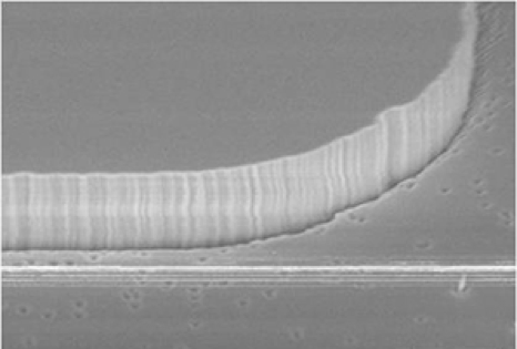
Process achieves anistropic profile and smooth surfaces .

More on RIE Request more information

Related Products