オックスフォード・インストゥルメンツー事業部ページ
Indium phosphide (InP) and its related compounds with Aluminium, Arsenide and Gallium forms the basis of many of the devices enabling the revolution in communication. InP is used in high-power and
high-frequency optoelectronics and electronics such as solid state lasers. Its superior electron velocity and direct bandgap result in fast switching optical components able to transmit huge amounts of data quickly. It can be etched using Inductively Coupled Plasma (ICP), Reactive Ion Etching (RIE) or Ion Beam Etch (IBE).
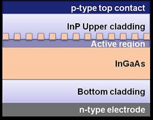
Example of InP based device:
buried Distributed Feedback (DFB) laser
Excellent profile control with smooth sidewall and etched surface at optimum etching rate.
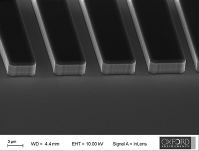
Using chlorinated process chemistries,
ICP-RIE is unrivalled for delivery of the precise profiles and smooth surfaces required for the critical InP Mesa/Ridge etch
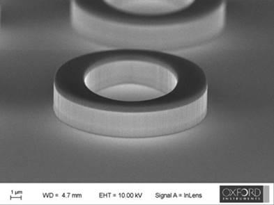
Excellent anisotropy and smooth surface. Accurate depth control.
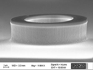
Excellent control of profile.

© オックスフォード・インストゥルメンツ 2026