オックスフォード・インストゥルメンツー事業部ページ
拡張

2D 材料

2D materials such as graphene, MoS2 or hBN can be used to enhance current devices and build new device architectures. FETs, batteries and filters with unique proporties can now be realised.  Oxford Instruments Plasma Technology offers precise process control for mono/multi layer growth with low defects.

Proven low damage results.

  • Temperature >800°C
  • Load-locked system offers higher throughput, as no cooling of the growth chamber is required to exchange samples
  • He purge gas is required for the process
  • Characterization of 2D materials is performed using techniques such as Raman spectroscopy and Photoluminescence to study structural and (opto) electronic quality.


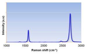
This specification is issued for Graphene obtained through Chemical Vapour Deposition (CVD) processes.

  • Load-locked system offers higher throughput, as no cooling of the growth chamber is required to exchange samples
  • He purge gas is required for the process
  • The presence of Graphene layer(s) will be tested by Raman Spectroscopy peak 2D analysis
  • 1 layer Graphene will be confirmed by Raman Spectroscopy
Request more information
  • Temperature 600°C - 900°C
  • Load-locked system offers higher throughput, as no cooling of the growth chamber is required to exchange samples
  • He purge gas is required for the process
  • Nucleation depends on the underlying substrate and C-source combination (Carbon, 2013, Vol. 58, 59–65)
Request more information

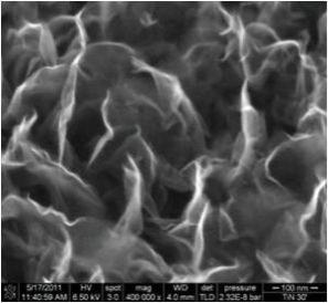
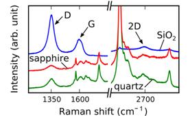
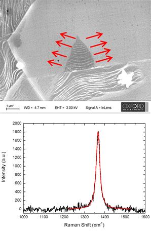
Direct growth of nanocrystalline Graphene on dielectric substrates using plasma enhanced chemical vapour deposition.

  • Temperature >900°C
Request more information

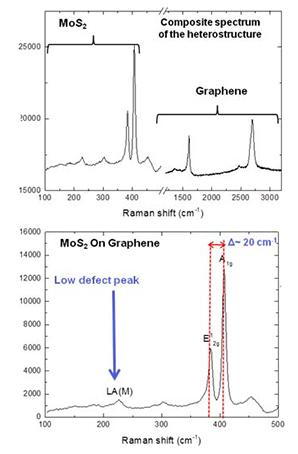
In situ growth of 2D Molybdenum Disulphide (MoS2) Graphene heterostructures

We offer CVD/PECVD/Remote plasma (ICP) CVD systems equipped with precursor vapour delivery modules for the growth of two dimensional layers and heterostructures of materials like Graphene, MoS2, WS2 etc. 

This is a three step process:

  • Step 1: Grow Graphene on Cu
  • Step 2: Transfer Graphene from Cu on to SiO2
  • Step 3: Grow MoS2 on Graphene transferred on SiO2

Process features:

  • Temperature >900°C
  • Formation of a single layer of MoS2 confirmed by Raman Spectroscopy
  • Deposition time is critical to ensure that a complete monolayer of MoS2 is formed
  • Temperature of MoS2 deposition on Graphene and its quality is critical for stability of the Graphene during MoS2 process
Request more information

This specification is issued for Boron Nitride obtained through Chemical Vapour Deposition (CVD) processes. For the purpose of process demonstration, B2H6 is used as Boron source and NH3 as the Nitrogen sources on Cu/Ni foils as catalyst substrates.

  • Temperature >900°C
Request more information

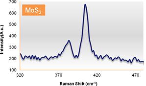
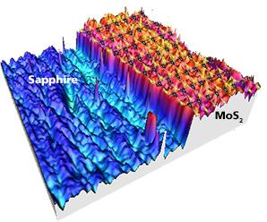
Growth of MoS2 and related 2D Transition Metal Dichalcogenides

We offer PECVD systems equipped with precursor vapour delivery modules for the growth of two dimensional layers of materials like MoS2, WS2 etc.

Excellent thickness control with low defects and strong  photoluminescence  

High quality MoS2:

  • AFM shows defined step height and smooth uniform film
  • Raman indicates one mono-layer is deposited with characteristic peaks spaced 21.1cm-1 apart
Request more information

Related Products