オックスフォード・インストゥルメンツー事業部ページ
Gallium Arsenide (GaAs) is commonly used in conjunction with Aluminium Gallium Arsenide (AlGaAs) to form mirrors in optoelectronic devices such as VCSELs. It is also forms part of the Multi Quantum Wells (MQWs) that are key to the performance of many devices. AlGaAs may be dry etched using Inductively Coupled Plasma (ICP), Reactive Ion Etching (RIE) or Ion Beam Etch (IBE). Etch processes can be either selective or non-selective to GaAs depending on the requirements.
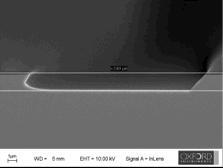
Excellent profile with low feature foot and smooth etched surface at high etching rate.
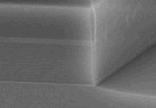
GaAs/AlGaAs may be etched using the Reactive Ion Etching (RIE) process. Excellent profile with low feature foot and smooth etched surface.
GaAs/AlGaAs multilayer etch
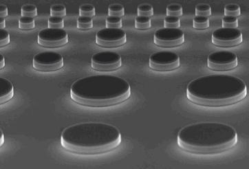
GaAs may be etched using the Reactive Ion Beam Etch (RIBE) process technique.
Competitive etching rate, selectivity and profile.

© オックスフォード・インストゥルメンツ 2026