オックスフォード・インストゥルメンツー事業部ページ
窒化ガリウム (GaN) は、いくつかの重要なテクノロジーにおいて重要な進歩を可能にする魅力的な材料です。GaNを使用した高輝度LED (HBLED) はすでに照明に革命をもたらし、またGaNレーザーダイオードは高速データ伝送に使用され、さらにGaNベースのRFデバイスは効率的な電力伝送と携帯電話基地局にまもなく適用されます。GaNは、誘導結合プラズマ (ICP)、反応性イオンエッチング (RIE)、イオンビームエッチング (IBE) などを用いてドライエッチングすることができます。また、 ALD を使用して成膜することもできます。
低ダメージで優れた表面粗さと最適化されたエッチングレートを実証するために、プロセスの専門知識が活かされています。
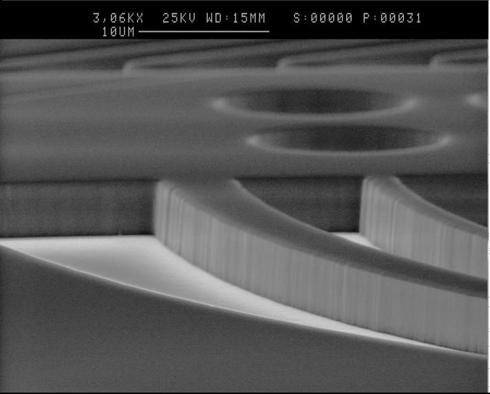
優れたエッチング速度で、異方性プロファイルを実現。

© オックスフォード・インストゥルメンツ 2026