オックスフォード・インストゥルメンツー事業部ページ
Al2O3 or Sapphire has many different applications. From Patterned Sapphire Substrates (PSS) for HBLEDs, gate dielectric on GaN HEMTs, wear resistant coatings and barrier layers it's hardness and electrical characterisitics make it the material of choice. It may be deposited using Atomic Layer Deposition (ALD) or Ion Beam Deposition (IBD). It can be etched using Inductively Coupled Plasma (ICP) and Reactive Ion Etching (RIE).
May be dry etched using the Inductively Coupled Plasma (ICP) process technique. High plasma density achieved high etch rate for tough materials. Patterned Sapphire Substrate (PSS) uses process expertise to demonstrate good heat control and achieve optimum feature height and excellent CD control.
Patterned Sapphire Substrate (PSS) Etch
Patterned Sapphire Substrate (PSS) uses process expertise to demonstrate good heat control and achieve optimum feature height and excellent CD control.
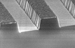
Ni masked Al2O3 features.
Patterned Sapphire Substrate (PSS) Etch
Excellent stoichiometry with competitive deposition rate. Etch source available for pre-clean.
Smooth etch surface and good control of etch depth.
Excellent material quality and low damage, even at low deposition temperature.
More on ALD Request more information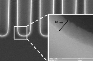
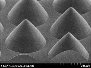
SEM image of a 80 nm remote plasma ALD Al2O3 film in 2.5 mm wide trenches with aspect ratio ~10 deposited in the FlexAL reactor, courtesy of Eindhoven University of Technology & NXP.

© オックスフォード・インストゥルメンツ 2026